
Outline & BIZ. Area
- Home
- Introduction
- Outline & BIZ. Area
SNS 공유하기


- Company Name
- P&L Semi Co.LTD.
- Business Area
- Semiconductor Wafer & Chip Design & Manufacturing / FAB. Foundry Service
- Establishment
- March19th,2015
- CEO
- Richard Goh
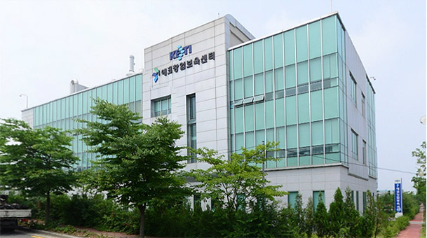
- Address
- B-207, 109, Ballyong-ro, Deokjin-gu, Jeonju-si, Jeonbuk-do, Republic of Korea
- Main Products
- Submount, Zener diode, photo diode, Transistor, LED, Silicon & Compound Based Semiconductor Device Design and Manufacturing
BIZ.Area
1Semiconductor Wafer & Chip Manufacturing
P&L semi production Capability is 6 inch 5,000 sheets wafer per month
2Foundry service
·Semiconductor Device Manufacture
Zener Diode
Sub mount
Photo Diode
Transistor
TVS Diode
·Semiconductor Foundry Service
Diffusion
Photo Lithography
Etch
Metalilzation
Die Saw
Visual Inspection
Device Design
Device Simulation
Chip Arrange
3Cooperated Overseas Company