2015
Founded
We continue to grow as a specialized optical semiconductor company.

Since 2015, we have designed and manufactured optical semiconductor devices and sensors through our own fab and R&D capabilities.
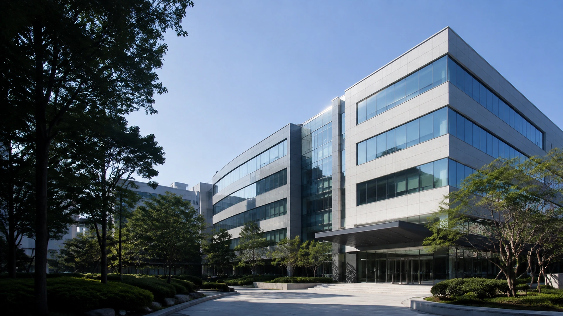
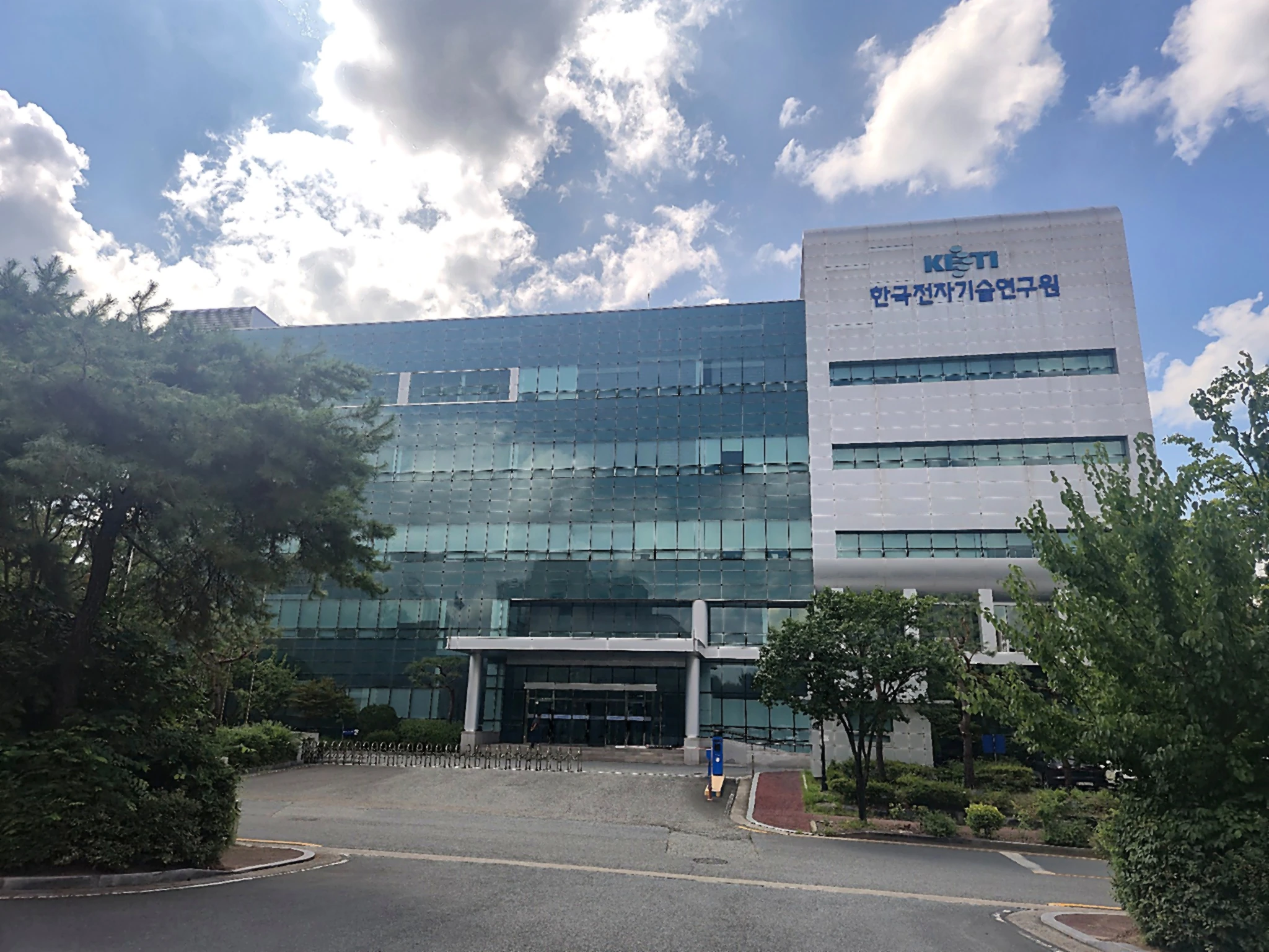
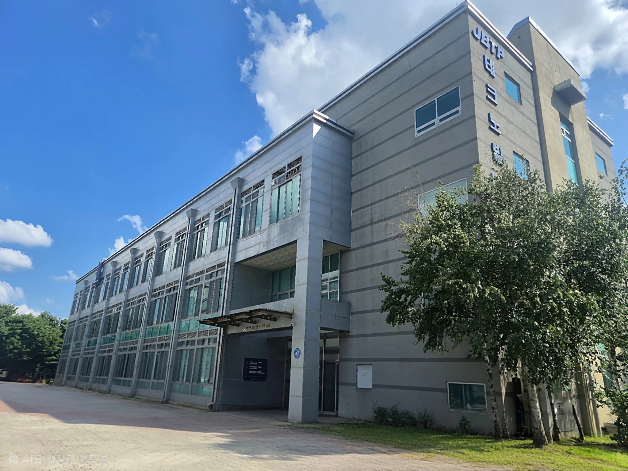
P&L SEMI operates its own fab at the KETI campus in Jeonju and performs key wafer and device processes in-house. Our broad product portfolio and quality systems support stable supply to customers worldwide.
We operate our own semiconductor fab at the KETI campus in Jeonju and perform major wafer and device processes directly.
We have a monthly capacity of 12,000 six-inch wafers and continue to expand production.
We design Photo Diodes, Zener Diodes, Submounts, APD Sensors, and UV Detectors in-house.
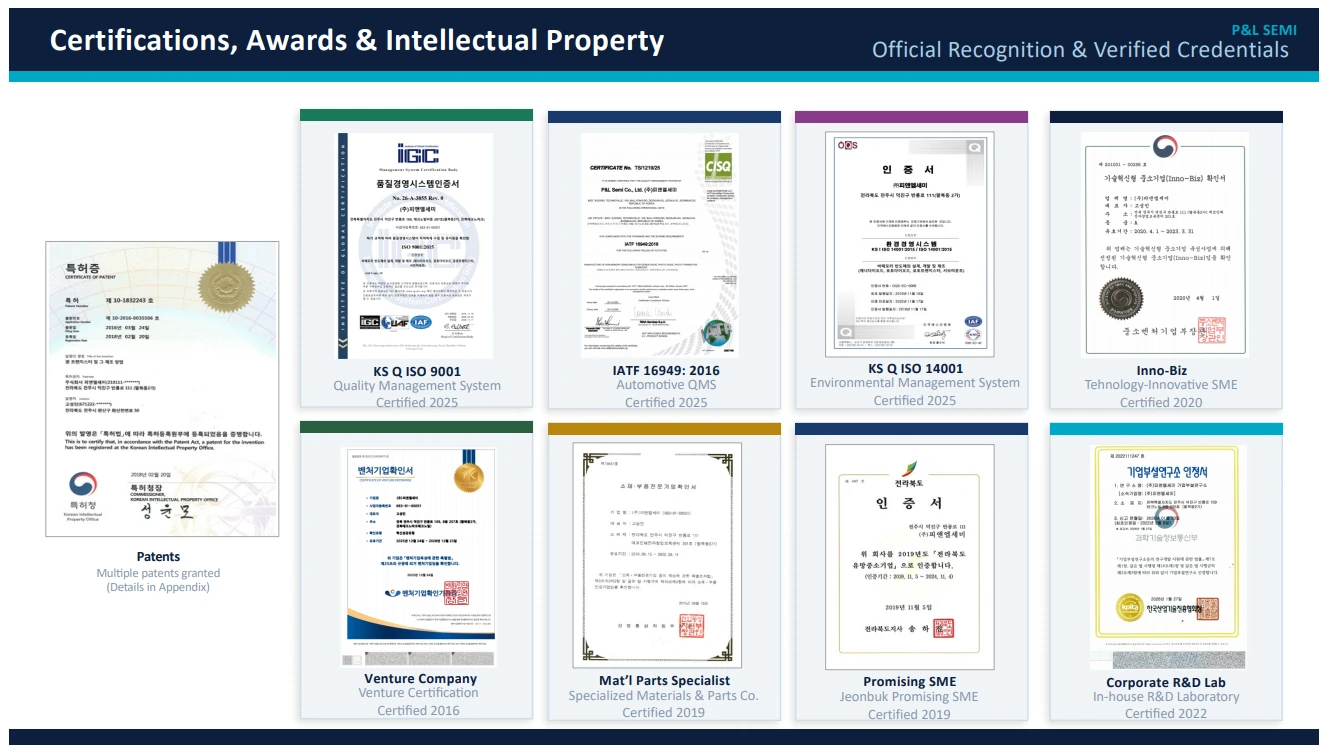
We operate staged IQC, PQC, and OQC quality control based on IATF 16949, ISO 9001, and ISO 14001.
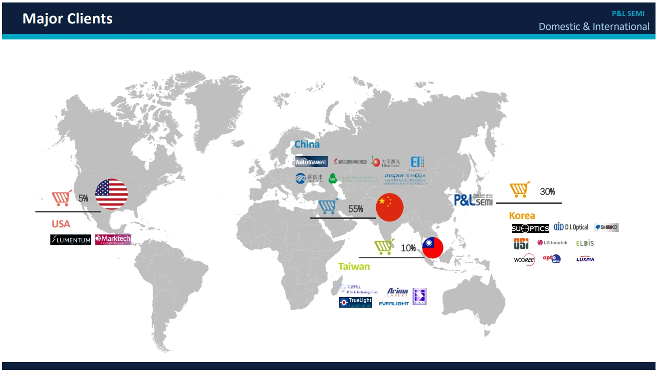
We serve more than 10 customers in Korea, China, Taiwan, and the Americas.
Our corporate R&D center advances APD, ROIC, and UV Detector technologies.
We established our semiconductor device business and began exports to Taiwan.
Mass production began for Zener Diodes, Submounts, Bidirectional Zeners, Flip-Chip Zeners, and Photo Diodes.
The company obtained specialized materials and components, Jeonbuk Promising SME, and Inno-Biz certifications while expanding production capacity.
P&L SEMI received the USD 5 Million Export Tower award, established a certified corporate R&D center, and expanded its APD and Photo Transistor businesses.
The company obtained IATF 16949 certification and continues developing next-generation products, including a single-channel LiDAR ROIC and UV Detector.
P&L SEMI works with customers in Korea, China, Taiwan, the United States, and other regions, maintaining stable long-term supply relationships.
Location information for customers and partners visiting P&L SEMI.