Technology

Own Fab
Integrated Process

Our own fab covers design, core wafer processes, and inspection to ensure stable quality and supply.

Precision wafer process technology
Technology Overview

INTEGRATED SEMICONDUCTOR MANUFACTURING

Integrated processes deliver
quality, speed, and stability.

From device design and wafer processing to inspection, P&L SEMI operates critical manufacturing processes in-house. Fast feedback between processes enables flexible response to customer requirements and consistent product quality.

In-house FabIntegrated ProcessFast Feedback
01

Wafer Process

Diffusion · Photolithography · Wet Process

Critical wafer process conditions are managed in-house.

02

Metallization

Metal Deposition · Patterning

Metal deposition and patterning are optimized for device performance.

03

Assembly

Grinding · Dicing · Packaging

Grinding, dicing, and assembly are connected in one production flow.

04

Inspection

Optical · Electrical · Reliability

Optical and electrical inspections verify outgoing quality.

Process Flow

From Design to Inspection One Integrated Process Flow

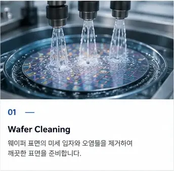
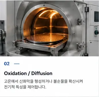
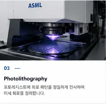
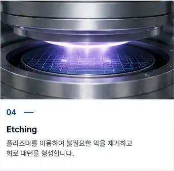
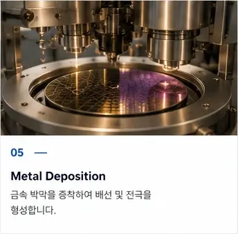
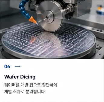
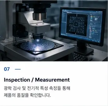
See P&L SEMI's semiconductor manufacturing flow through process-stage images.
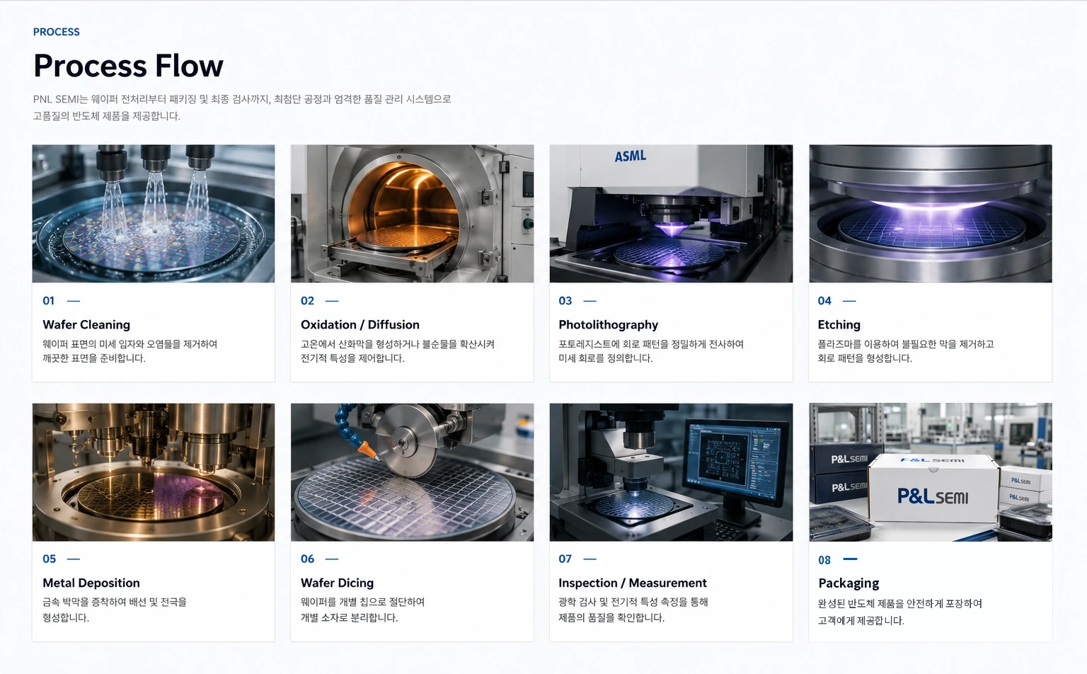
P&L SEMI semiconductor manufacturing process flow, steps 01 through 08
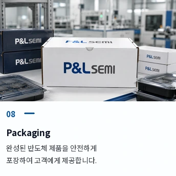
01 Wafer Cleaning 02 Oxidation and Diffusion 03 Photolithography 04 Etching 05 Metal Deposition 06 Wafer Dicing 07 Inspection and Measurement 08 Packaging
Quality Management

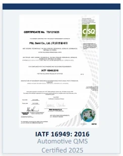
IQC → PQC → OQC Three-stage Quality Control

Quality is checked from incoming inspection through production and shipment, with customer feedback applied to continuous improvement.
IQC

Incoming Quality Control

  • Raw material inspection
  • Wafer substrate check
  • Supplier certification verification
  • Incoming specification compliance
PQC

Process Quality Control

  • In-line process monitoring
  • Dimensional checks at each step
  • Yield tracking per lot
  • SPC statistical control
OQC

Outgoing Quality Control

  • Final visual inspection
  • Electrical characteristic test
  • Spec conformance check
  • Packaging and label verification
CAPA

Continuous Improvement

  • Customer complaint intake
  • Root cause analysis
  • CAPA implementation
  • Feedback loop to IQC/PQC
Technology Partnership

Customized Semiconductor Devices and Processes for Customer Needs.