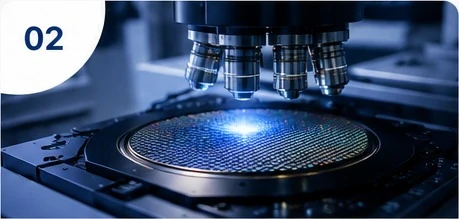
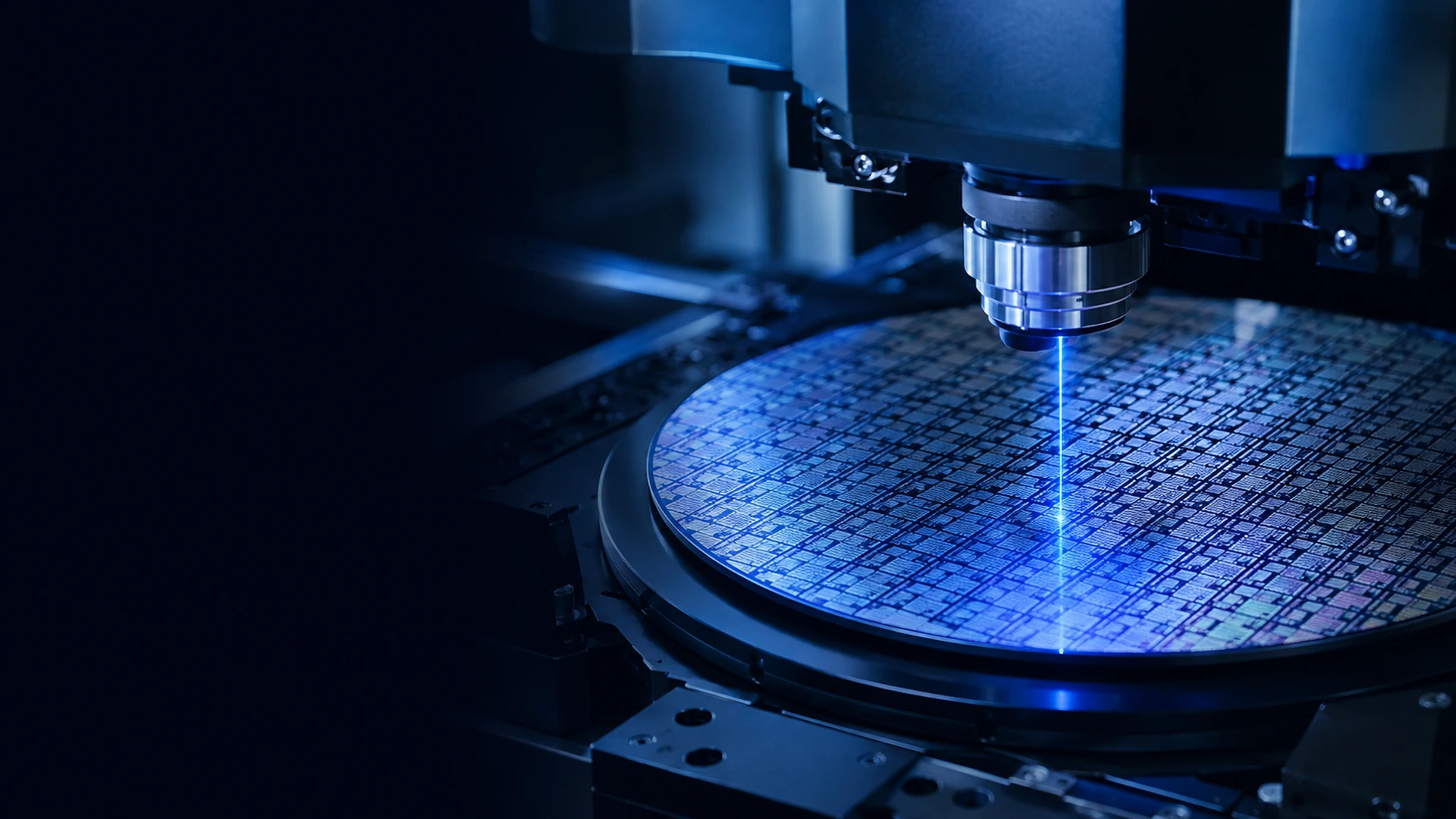
Precision equipment inspecting a semiconductor wafer
P&L SEMI · PRECISION TECHNOLOGY

Creating the Future with
Light and Semiconductor Technology.

We enhance customer competitiveness through optical semiconductor devices, sensors, and precision packaging technology.

01/ 03
Our Principles

Technology Begins with Trust.

We create new value through customer focus, quality, and innovation.

Our Products

P&L SEMI Core Products

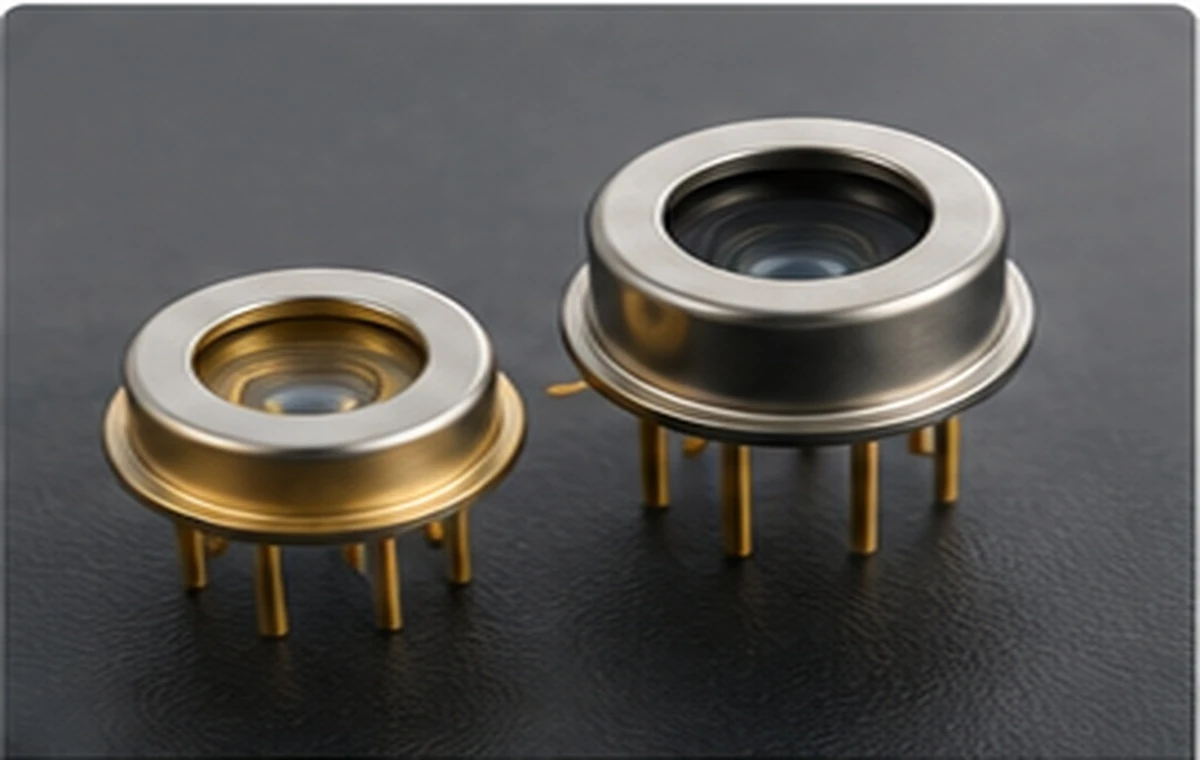
Explore our optical semiconductors, sensors, protection devices, and precision submounts.

Manufacturing Capability

Reliable Supply through
Our Own Fab and Process Technology.

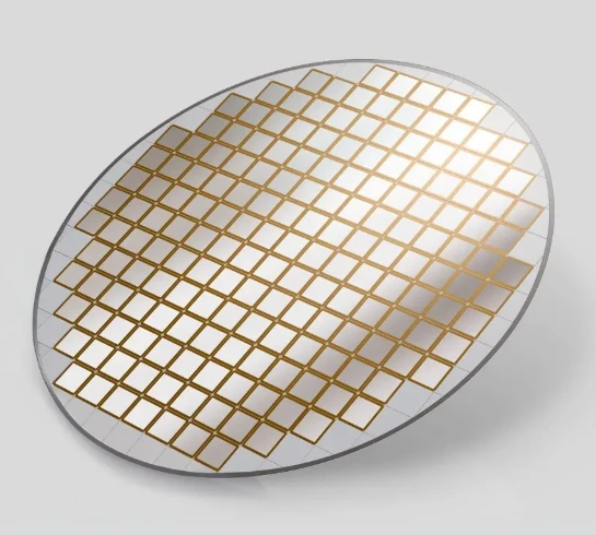
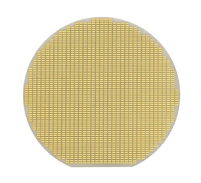
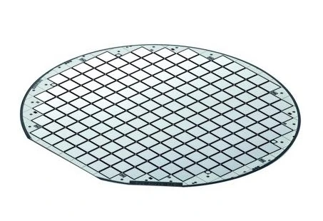
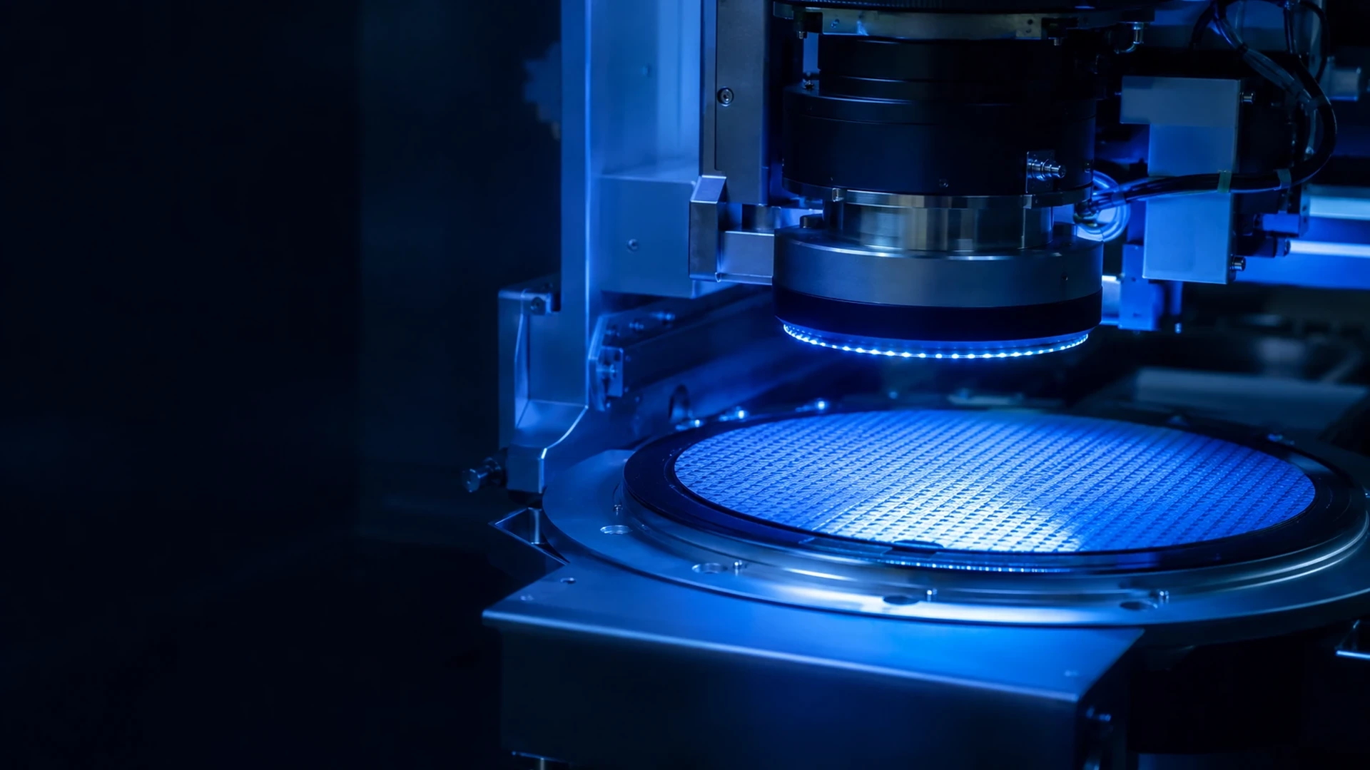
We directly operate key semiconductor processes from design and diffusion to photolithography, metallization, dicing, and inspection.

12K6-inch Wafers / Month
98.5%Production Yield
10+Domestic & Overseas Customers
Custom Semiconductor Solution

From Requirements to Production,
One Integrated Process.

We review each application and specification, then support the entire journey from device design and own-fab production to inspection and reliable supply.

  1. 01

    Requirement Review

    We define the application, wavelength, sensitivity, voltage, size, and other key requirements.

  2. 02

    Device Design

    We design the device structure, materials, pads, thickness, and target characteristics.

  3. 03

    Own-Fab Production

    Core wafer processes and precision packaging are performed in our own fab.

  4. 04

    Quality & Delivery

    Electrical and optical characteristics are verified before stable delivery.

Contact Us

Building a Better Semiconductor Future Together.

Contact Us